Services

- Details
- Category: News
- Published on Friday, 10 July 2015 14:45
- Written by Super User
- Hits: 13533
Sell microcantilever (Si Substrate)
*Price is open for negotiation

Array microcantilever sample

cantilever 1 : width ~ 40 um
cantilever 3 : width ~ 20 um
ADVANCED HYDROPHOBIC NANOLAYER FOR MEMS APPLICATION
~ Service Price RM 200/hour
sample

Handphone only

Handphone + MVD

Hydrophobic Nano Layer
ADVANTAGE
- Low thermal damage (low temperature process)
- Process control through automation
- Excellent production repeatability
- Demonstrated large yield increase
- Demonstrated product enablement
- Safe operation
- Applicable to many materials
- High precision
- Low cost
- Only 2 MVD machines in Malaysia
MEMS STRUCTURE REALIZATION USING KRF EXCIMER LASER MICROMACHINING
~ Service Price RM 0.01/firing

sample:

Piezoresistor mask & fabrication structured by micromachining
ADVANTAGES
- Appropriate cost
- Can design a micro size in short period of time
- Environmental friendly
- Less chemical usage especially in etching process
- Reduce the number of mask involves
- Applicable to many materials
- Highly flexible CNC programming
- High precision (tolerance ± 1um)
- Low thermal damage
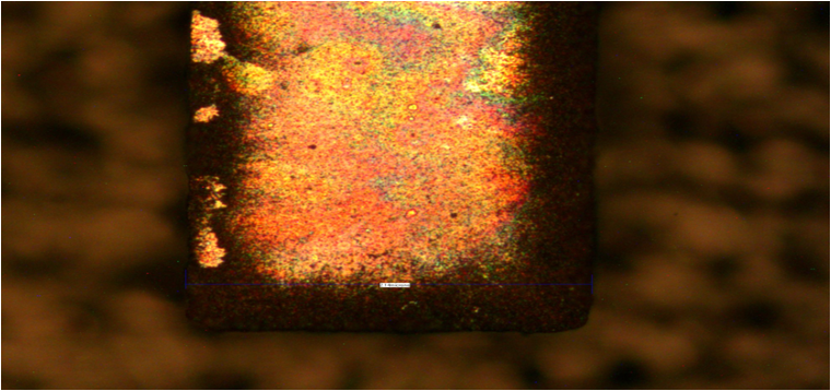
APPLICATION OF ADVANCED ANHYDROUS HF BASED SACRIFICIAL SIO2 REMOVAL TOWARDS ANTI-STICTION MEMS REALIZATION
~ Service Price RM 200/hour

sample

Sample 1: Etch/Remove oxide layer on silicon wafer
ADVANTAGE
- Know how to optimize Silterra HF vapor release process recipe.
- Realization of MEMS structure on Silterra CMOS substrate
- Can etch sacrificial SiO2 and other films
- Eliminates stiction – dry vapour process, repeatable, controlled
- Reduce pressure & elevated pressure
- Fast process & low cost
- Compatible with many metals/typical MEMS materials (Al)
- The graduate intern can be absorbed as the worker of the collaborating organization
- Recognition to the academician